GY-BMP280 - Bosch BMP280 high-precision and low-power digital barometer
Contents:
- Description
- Wiring Connections
- Electrical Specifications
- Pinouts
- i2c device permissions
- Raspberry Pi Code Example
- Description
- Wiring Connections
- Electrical Specifications
- Pinouts
- i2c device permissions
- itbrainpower.net
- References
[Top][Home]
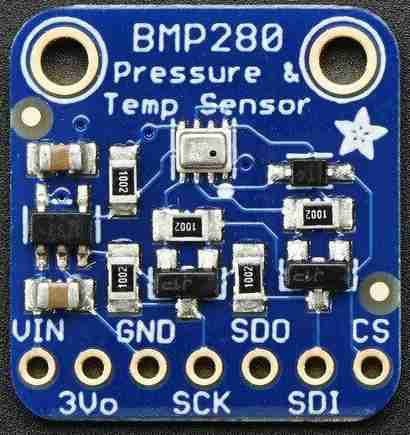
The Adafruit Module:
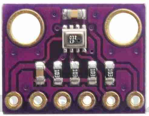
The generic Module (Front and Rear):
[Top][Home]
Description
The GY-BMP280 module operates from 3.3V so requires 3.3V power and must be
driven with 3.3V logic levels. If needed to operate at 5V, it can be done using
voltage regulator and level shifters as it doesn’t contain one. It is typically
recommended to operate it on 3.3V and maximum at 3.6VDC. The module GY-BMP280
module simply supports both I²C and SPI interfaces and comes with default I²C
address of 0x76. The Chip Select (CSB) and Serial Data Output (SDO) pins of the
BMP 280 are necessary only when SPI-based (four-wire) communication is applied.
I2C is a two wire interface SDA SCK.
Leave pin 6 of the module (SDO) unconnected to set the I²C address to 0x76 –
the on-board resistor pulls the SDO pin low setting the address to 0x76.
To change the I²C address to 0x77, connect pin 6 of the module (SDO) to Vcc
which would typically be the 3.3V supply.
Pin 5 of the module (CSB) must be connected to Vcc to select the I²C interface.
This is already done by an on-board pull-up resistor, so pin 5 can be left
disconnected when using the I²C interface.
[Top][Home]
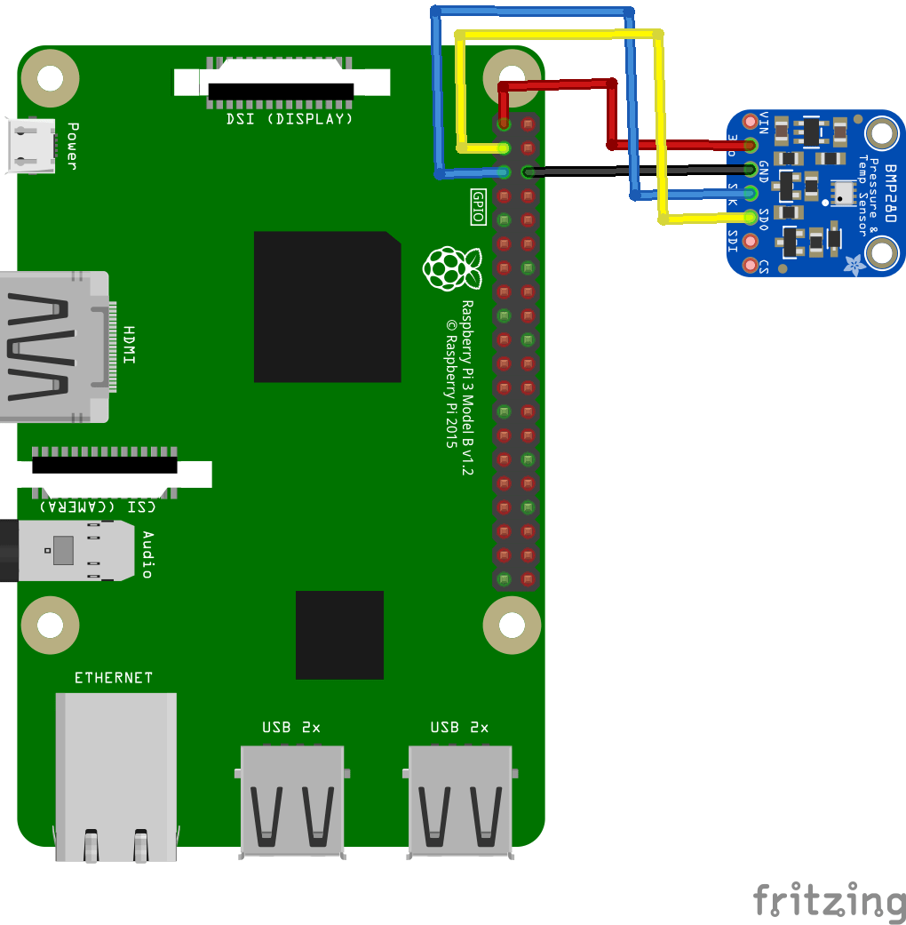
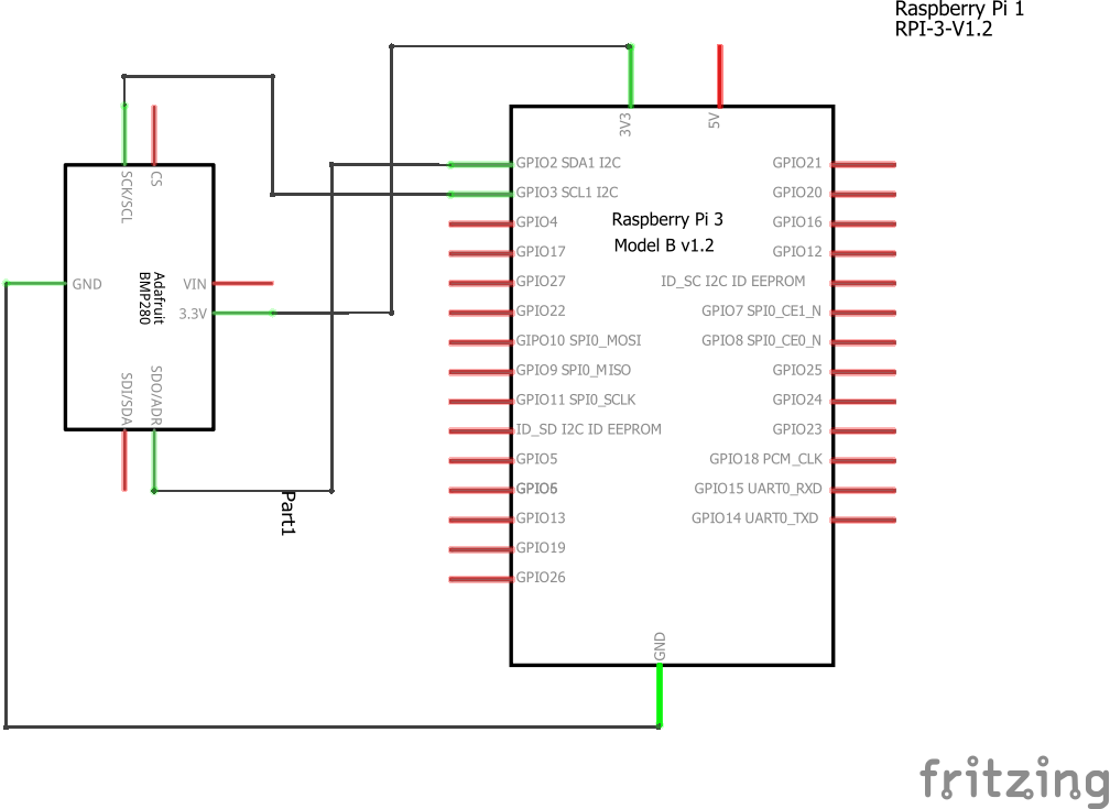
Wiring Connections
PIBITS - RASPBERRY PI AND BMP280 SENSOR EXAMPLE:
[Top][Home]
Electrical Specifications
- Model: GY-BMP280-3.3
- Chip: BMP280
- Power supply: 3V/3.3V DC
- Peak current: 1.12mA
- Air pressure range : 300-1100hPa (equi. to +9000…-500m above sea level)
- Temperature range: -40 … +85 °C
- Digital interfaces: I²C (up to 3.4 MHz) and SPI (3 and 4 wire, up to 10 MHz)
- Current consumption of sensor BMP280: 2.7µA @ 1 Hz sampling rate
[Top][Home]
Pinouts
| Pin No. | Pin Name | Pin Description |
| 1 | VCC | Power source of 3.3VDC |
| 2 | GND | Ground |
| 3 | SCL | Serial Clock |
| 4 | SDA | Serial Data |
| 5 | CSB | CSB pin to GND to have SPI and to VCC(3.3V) for I2C. It’s an input to the chip. |
| 6 | SDO | Serial Data Out / Master In Slave Out pin, for data sent from the BMP280 to your processor |
[Top][Home]
i2c device permissions
wget -O bme280.py http://bit.ly/bme280py
[Top][Home]
Raspberry Pi Code Example
[Top][Home]
itbrainpower.net
RaspberryPI BME280 / BMP280 sensor how to:
https://itbrainpower.net/a-gsm/RaspberryPI-BME280-or-BMP280-sensor_howto
[Top][Home]
References
BOSCH - Digital Pressure Sensor:
https://www.bosch-sensortec.com/media/boschsensortec/downloads/datasheets/bst-bmp280-ds001.pdf
https://www.raspberrypi-spy.co.uk/2016/07/using-bme280-i2c-temperature-pressure-sensor-in-python
GY-BMP280-3.3 Pressure Sensor Module Arduino Tutorial - Created on: 27 March 2018:
https://startingelectronics.org/tutorials/arduino/modules/pressure-sensor/
[Top][Home]
Glenn Lyons VK4PK
glenn@LyonsComputer.com.au
Ver:gnl20201204 - pre published v0.9